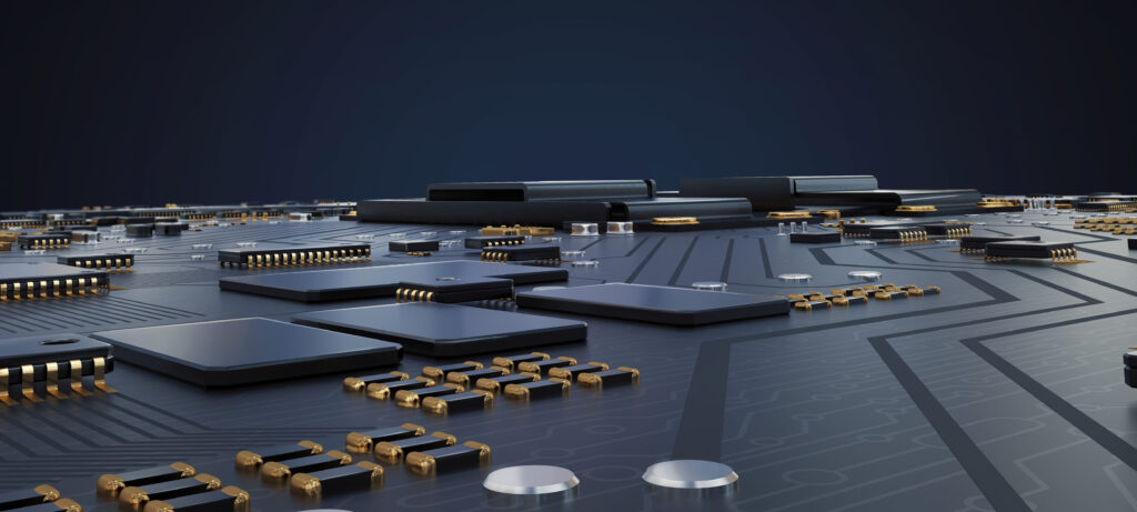
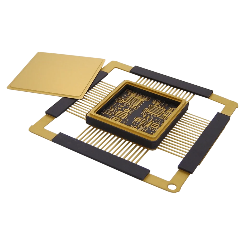
The microelectronics industry demands precision and expertise, so they turn to Photofabrication Engineering, Inc. (PEI) for their most essential products, including step lids, flat lids, lids with getters, Lead Frames (semiconductor/glass-to-metal seals), etched carriers, carriers with solder dams, circuit stators, and many others.
Microelectronics is an industry that touches nearly every aspect of our lives, so ensuring that experts craft every part and component is crucial.
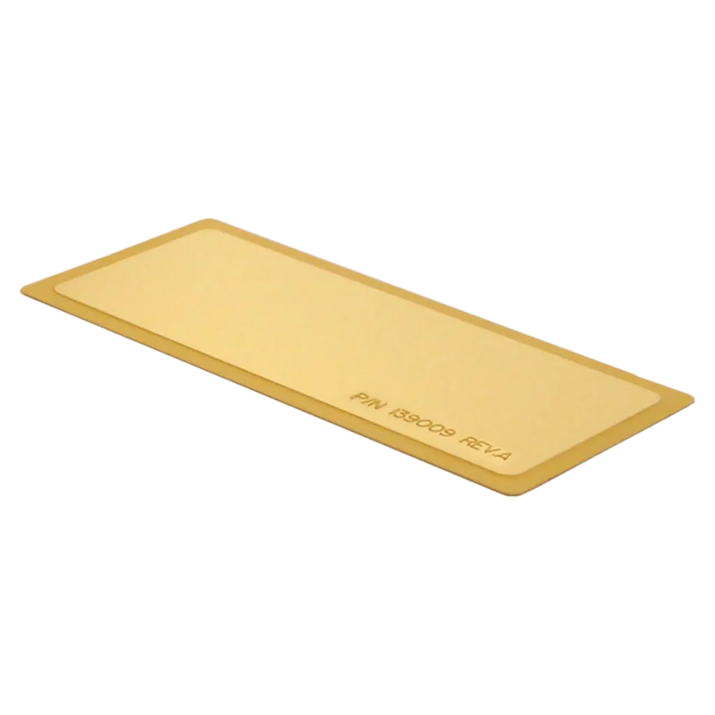
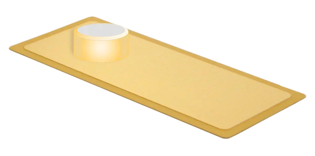
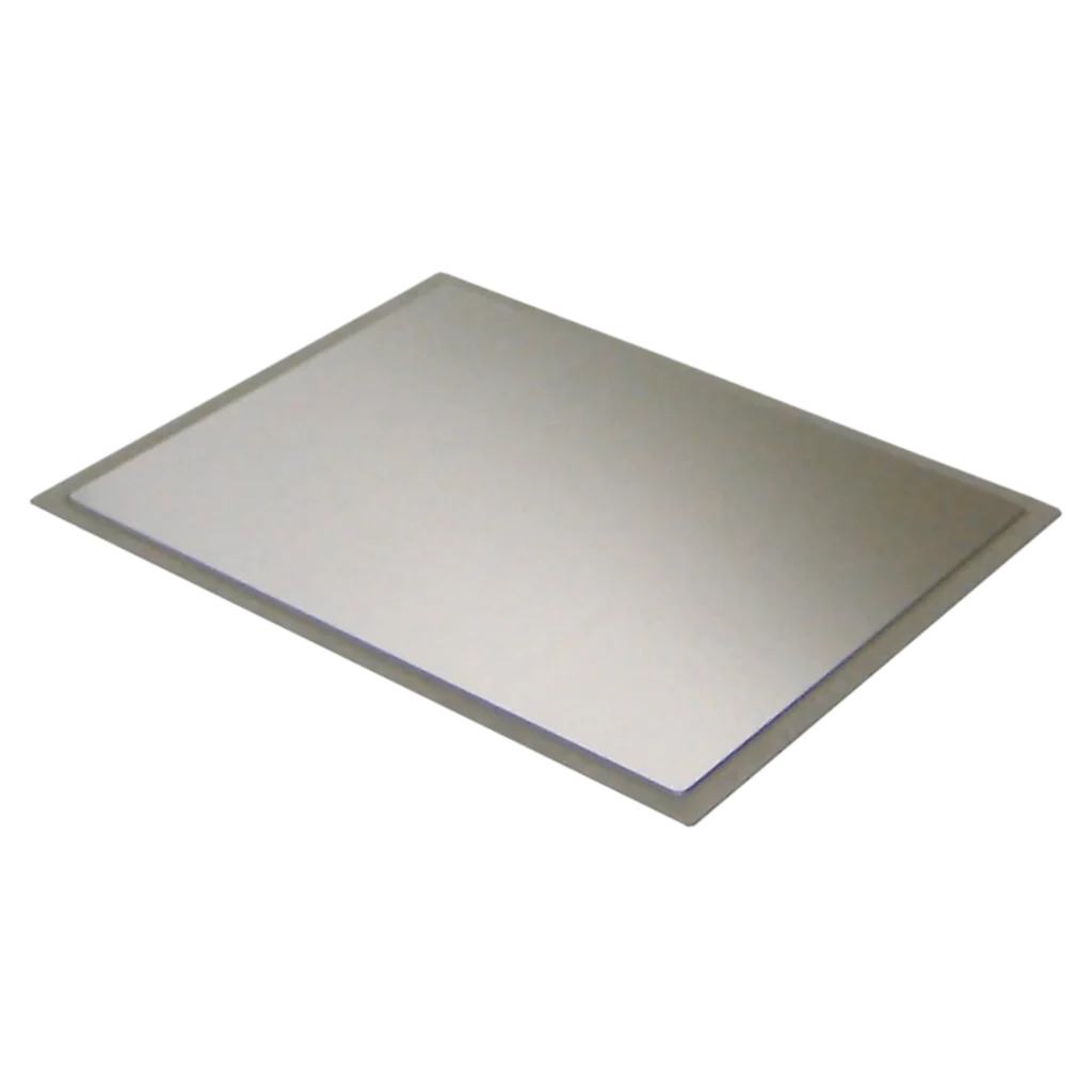
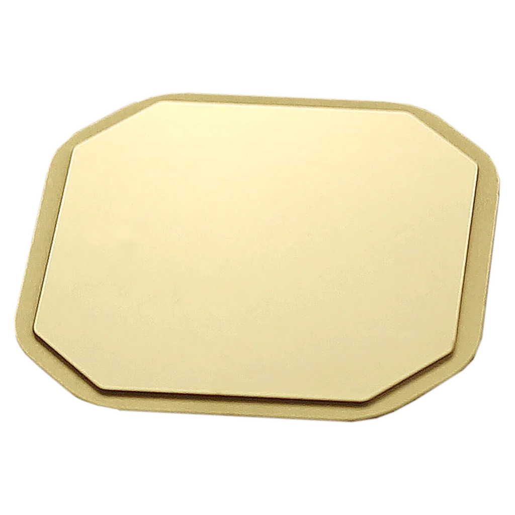
To meet the industry’s needs, PEI established a department dedicated to producing custom and standard Step Lids & Flat Lids for seam-weldable microelectronic packages, including lids with getters for hydrogen and moisture absorption.
PEI leverages the power of photochemical etching, a manufacturing process that produces burr-free parts in intricate geometries essential in precisely fabricating step lids. PEI’s microelectronic products meet and exceed the most stringent requirements such as ROHS, ITAR & DFARS.
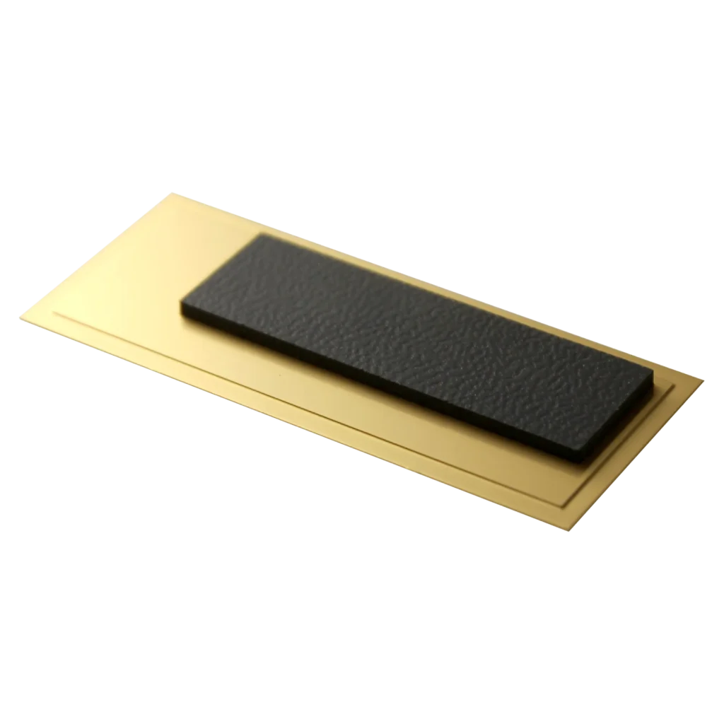
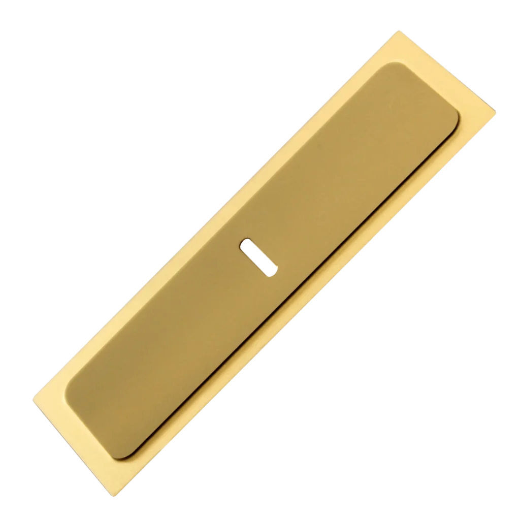
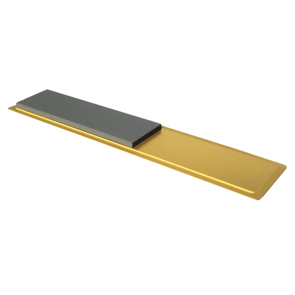
PEI produces a full line of custom and standard step and flat lids for seam-weldable microelectronic packages. We can also provide these lids with getters that are either screened on or applied with other methods. These getters absorb moisture or residual hydrogen after hermetic package closure.
Package and hybrid manufacturers may purchase lids to a given print or specify the package to which the lid will be welded. We will gladly assist in designing a custom lid solution to ensure optimum yields and lid closure. These custom lids are available with a one-time tooling charge, which may be absorbed on large-volume orders.
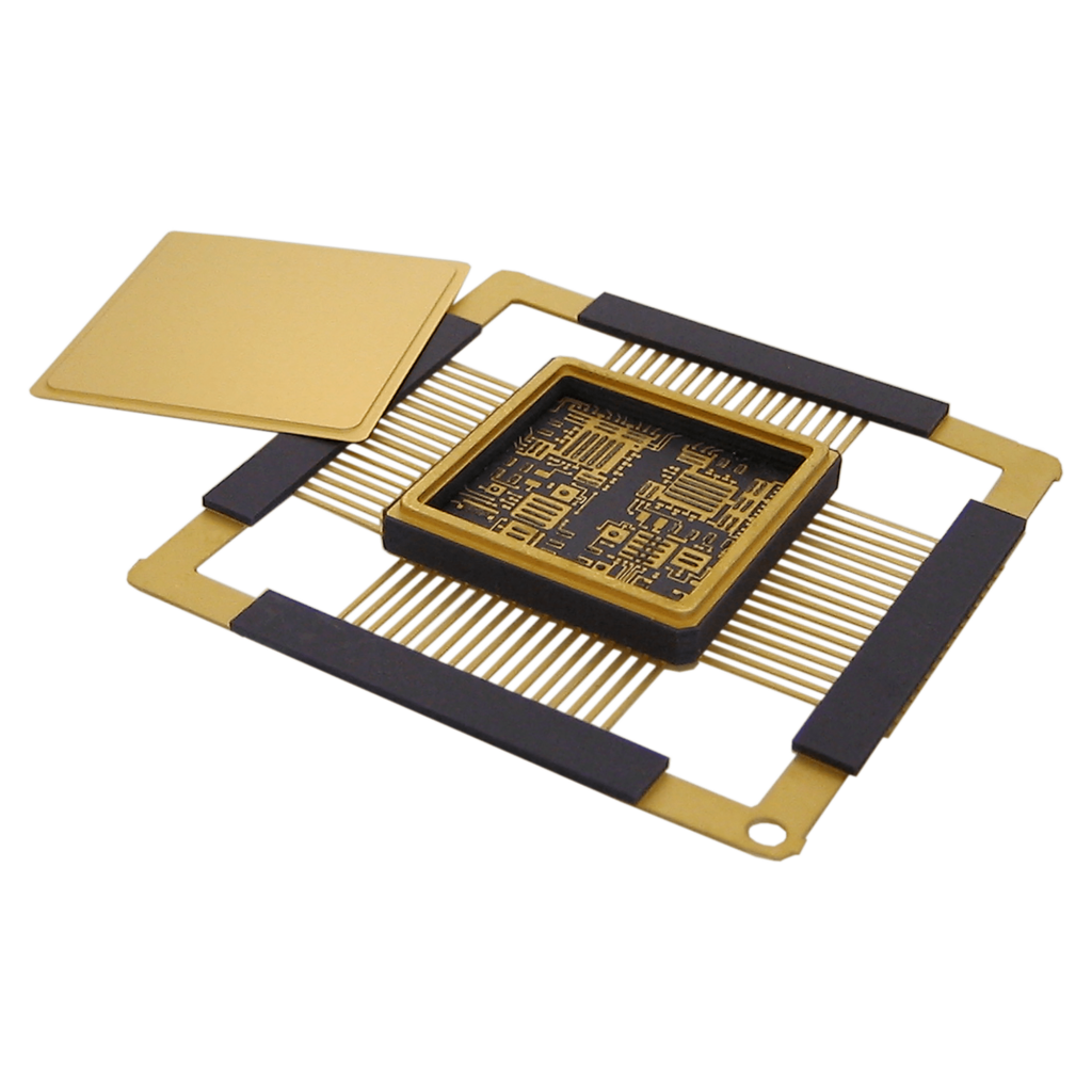
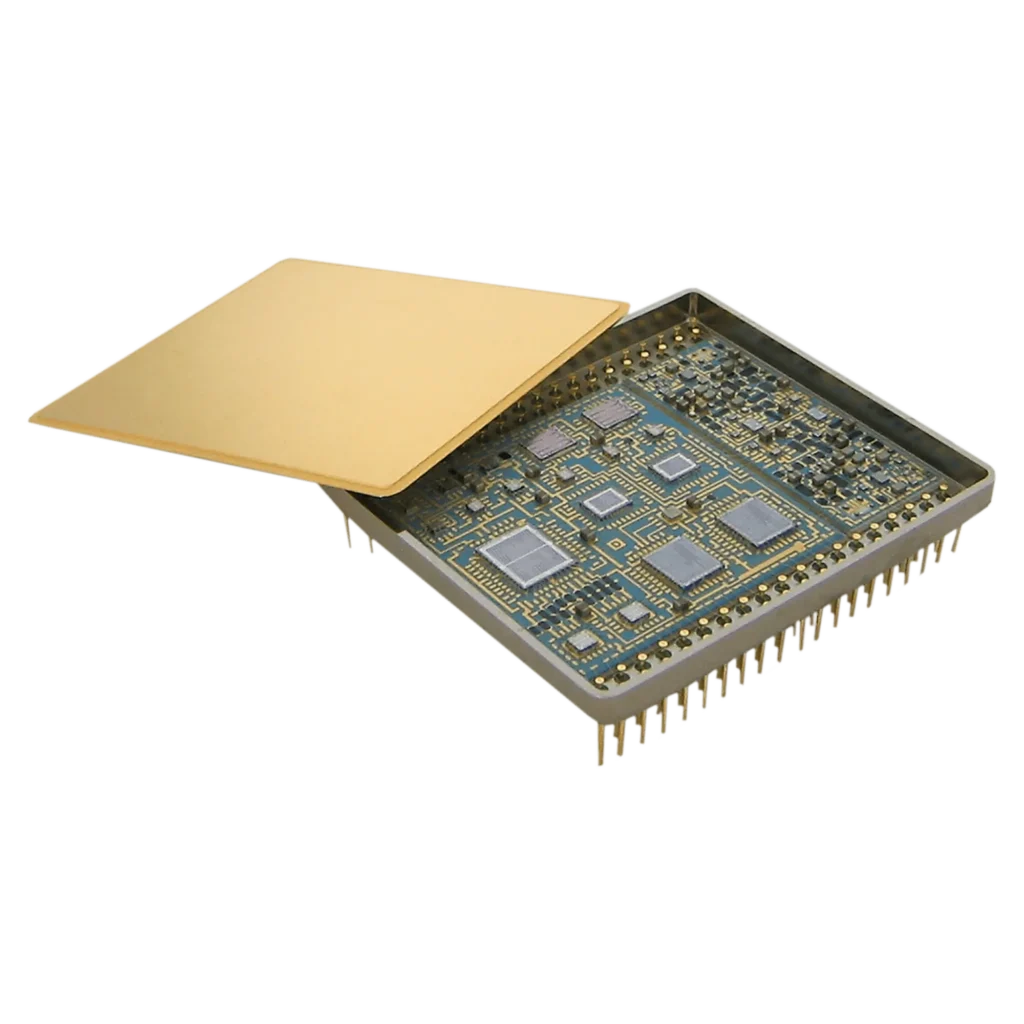
A step lid is a precisely fabricated component that provides protection and hermetic sealing for microelectronics and sensitive electronic devices. A step lid features a unique profile where the top plate is wide and the base is narrow to fit into the top, making a solid package.
In addition to mechanical protection and hermetic sealing, engineers design step lids to dissipate the heat produced by the enclosed components. Depending on the specifications, manufacturers often finish step lids with gold plating, electrolytic nickel plating, or electroless nickel plating.
There are various factors to consider when selecting what material to use for step lids. The choice of material often depends on an engineer’s specifications and the demands of the microelectronic.
Our standard base material for lids is etching-grade iron-nickel cobalt alloy, but our experts are here to walk you through your options. We’ve used the following metals for step lids:
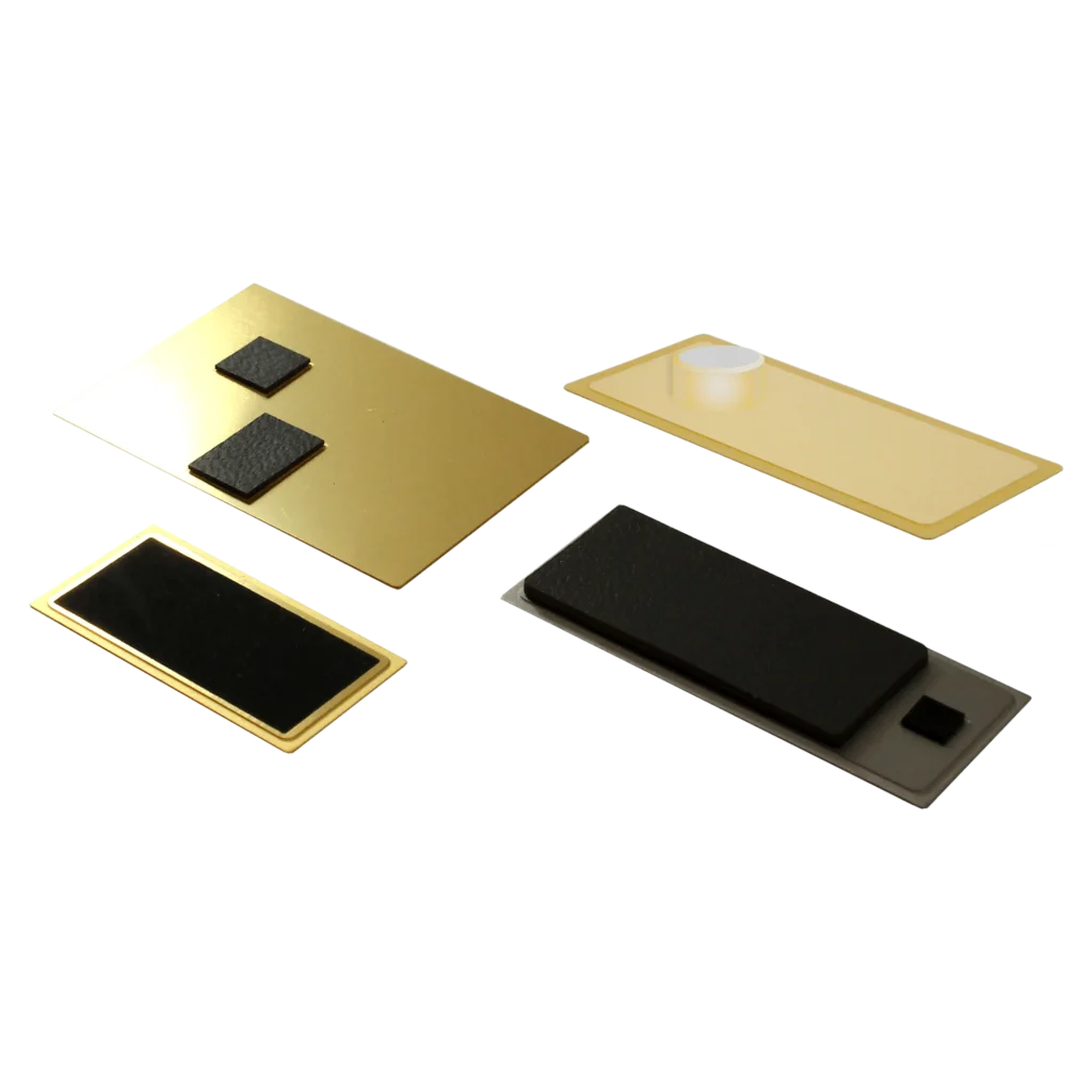
Step lids can be found in nearly every industry because microelectronics are such an essential part of the technology and machinery in our daily lives. PEI has more than 50 years of experience producing step lids for electronics, aerospace and defense, and medical customers.
Key applications include:
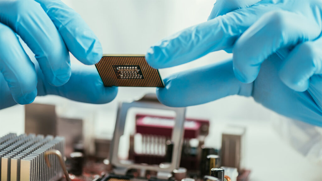
Step lids enable the hermetic sealing of sensitive electronic components while protecting those essential microelectronics from moisture, gasses, and contaminants.

Microelectronics used in aerospace and defense applications face harsh environments and extreme conditions. Step lids offer protection from both by adding stability.

Step lids can be found in implants and medical devices and offer a durable and sterilized solution while protecting sensitive electronics.

Photochemical etching, also known as precision chemical machining, chemical blanking, or acid etching, is an exact subtractive manufacturing process where chemical etchants selectively remove metal from a thin sheet to create intricate shapes, patterns, and features. Unlike traditional methods, photochemical machining does not involve mechanical force or direct contact with the sheet of metal, minimizing the risk of distortion, burrs, or stress-induced deformation.
The benefits of photochemically etching step lids include fabricating precise parts with intricate geometries and accurate patterns.
Here are additional benefits of titanium photochemical etching:
With a history of engineering excellence, PEI is among the top companies providing photochemically etched metal parts and components for various critical industries.
With ISO-9001:2008 and AS9100 certifications, PEI was also granted certification under the International Traffic in Arms Regulation (ITAR) in 2010, enabling it to provide weapon system components and accessories in compliance with the Code of Federal Regulations implemented by the U.S. Department of State.
Our rigorous inspection processes and testing procedures ensure that every product we produce meets stringent accuracy, reliability, and performance standards.
