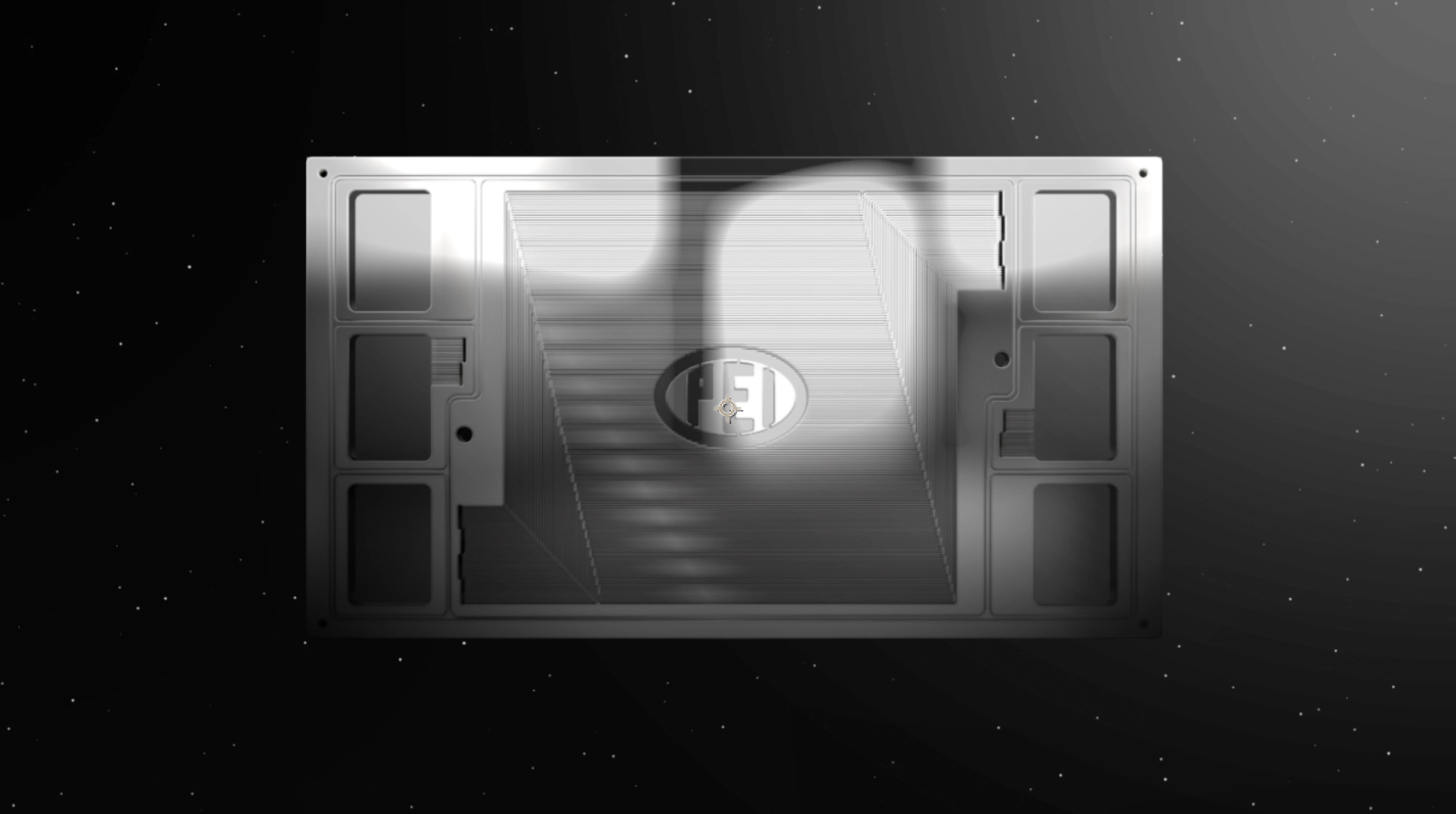
PEI’s precision photochemical machining capabilities are built around delivering highly accurate, repeatable thin metal parts for aerospace, medical, electronics, defense, and industrial applications.
Our advanced photochemical machining workflow combines engineering expertise, process control, and decades of innovation to produce precision components with tight tolerances, complex designs, and exceptional material integrity.
Unlike conventional fabrication methods such as laser cutting or stamping, the photochemical etching process removes material chemically rather than mechanically. This preserves the metal’s grain structure while producing burr-free parts without introducing stress or heat distortion.
The photochemical machining process is a carefully controlled, multi-step process in which each stage directly affects final part quality, dimensional accuracy, and repeatability.
While every manufacturer approaches photochemical machining differently, PEI has developed proprietary methods and advanced process controls that optimize precision, consistency, and manufacturing efficiency.
The first stage of the photoetching process begins with engineering and photo-tool development.
The PEI engineering team works directly with customer CAD files to optimize each desired part for the unique characteristics of photochemical machining. During this stage, engineers evaluate process variables such as:
Because material is removed chemically from both sides of the coated metal, engineers must compensate for lateral and surface etching to ensure finished parts meet exact specifications.
Once optimized, the CAD image is arrayed across the metal sheet to maximize yield and manufacturing efficiency. Depending on part complexity and requirements, the image is either exported directly using LED imaging systems or produced onto film to create the photo tool used during exposure.
Precise registration between top and bottom tooling is essential for maintaining alignment accuracy throughout the PCM process.
Before the photochemical etching process can begin, the bare metal must be carefully cleaned and prepared.
Material preparation removes:
This ensures the photoresist properly adheres to the metal surface during subsequent operations.
PEI was the first company in the photo chemical machining industry to transition to a solvent-free facility, replacing harsh degreasing chemicals with environmentally responsible cleaning systems. Today, most coated metal and bare metal sheets move through a multi-stage cleaning system utilizing high-pressure rinsing, mild cleaning agents, and deionized water preparation.
Different materials may require specialized preparation techniques depending on their chemistry, thickness, and application requirements.
Following cleaning, dry-film photoresist is laminated onto the coated metal using a precision hot-roll lamination system.
We exclusively use dry-film photoresist because it offers:
The coating stage occurs in a controlled, safe-light environment to prevent premature exposure to UV light.
Depending on material thickness and application, we can process either individual sheets or coil-fed materials through the etching line. Excess resistance is trimmed after coating to prepare the material for imaging and exposure.
Our expert team leverages advanced ALTIX LED imaging systems and precision contact printers to transfer the component design onto the photoresist.
During imaging, UV light exposes selected regions of the photoresist according to the digital artwork or photo tool design. Exposed areas harden while unexposed regions remain soluble during development.
For contact printing applications, two pieces of film sandwich the metal sheet, while vacuum pressure removes air gaps and ensures intimate contact between the tooling and the material. This helps maintain extremely tight tolerances and imaging accuracy.
Our state-of-the-art clean room environment helps prevent contamination and ensures repeatability across every production run.
Once exposure is complete, the coated metal moves into the developing stage of the photochemical machining workflow.
During development, high-pressure alkaline chemistry removes the unexposed photoresist, revealing the bare metal areas to be etched while leaving hardened resist behind to protect the desired geometry.
This stage creates the durable, patterned mask necessary for accurate chemical milling and prepares the part for final etching.
Our conveyorized developing systems help maximize production capacity while maintaining consistent process control across the entire manufacturing process.
The actual etching process occurs when prepared metal sheets enter our conveyorized chemical milling systems.
During this stage, specialized etchants spray both sides of the metal sheet simultaneously, dissolving exposed material while protected regions remain intact beneath the hardened photoresist.
We carefully monitor critical process variables, including:
Maintaining tight control over these variables allows our team to produce parts with highly accurate feature geometry and repeatable dimensional tolerances.
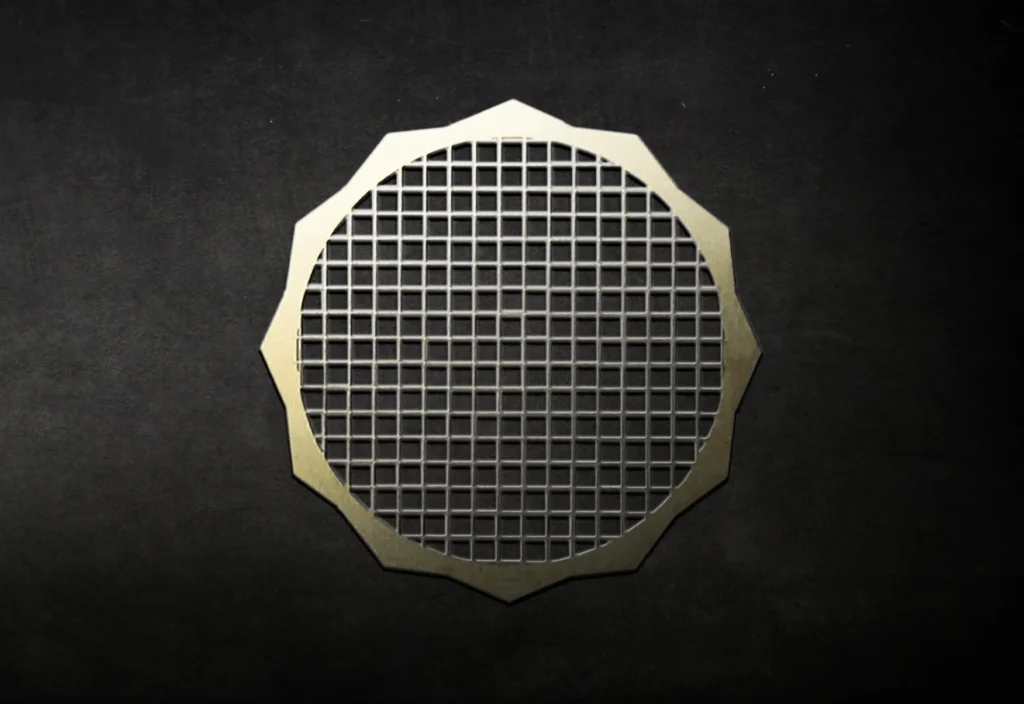
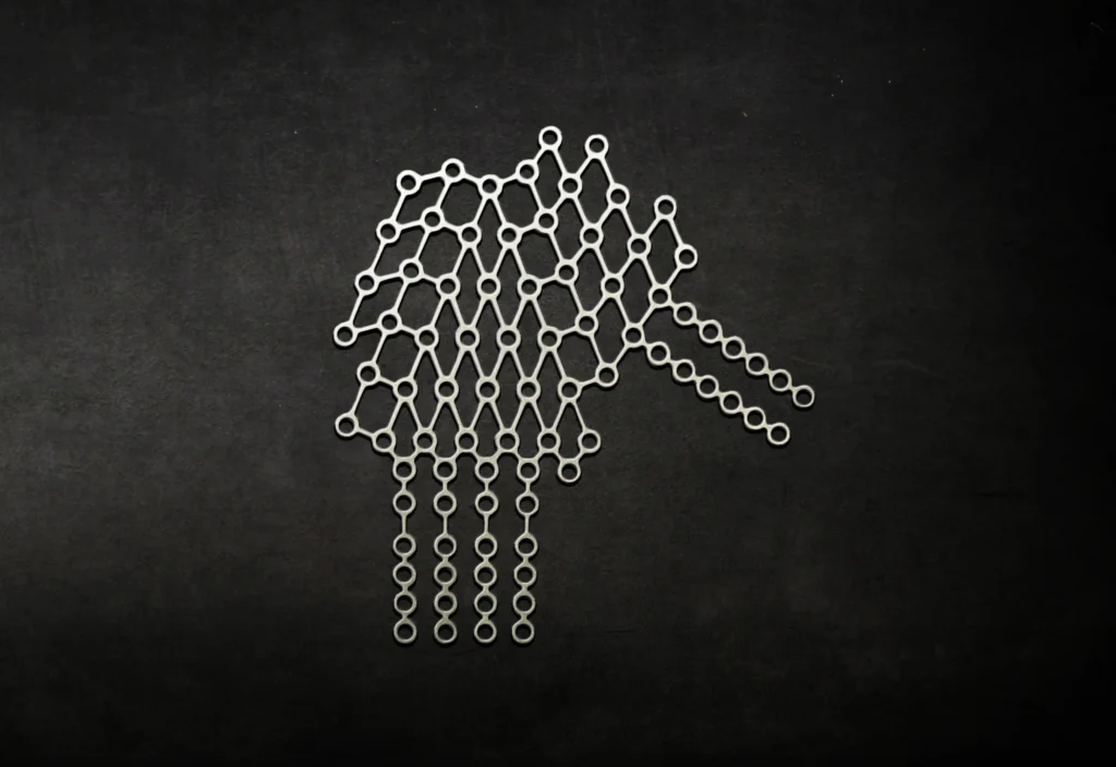
Because photochemical machining removes material uniformly without mechanical force, it produces thin metal parts with smooth edges and exceptional precision.
We continue investing heavily in advanced etching equipment and chemical management technologies to expand manufacturing capacity and improve process efficiency.
After etching is complete, the remaining photoresist must be removed from the parts.
We use conveyorized stripping systems to dissolve the hardened resist and clean the metal surface thoroughly. Once stripped, parts are rinsed using deionized water and dried before inspection, or post-processing operations begin.
At this stage, parts produced through photochemical machining are ready for:
Photochemical machining offers several advantages over other processes used to manufacture precision metal components.
The PCM process enables highly accurate feature definition and repeatable dimensional control across complex designs.
This makes photochemical machining ideal for:
Unlike laser cutting or stamping, the photochemical etching process introduces no heat-affected zones or mechanical distortion.
This allows our team to produce burr-free parts while preserving the original grain structure and magnetic or mechanical properties of the material.
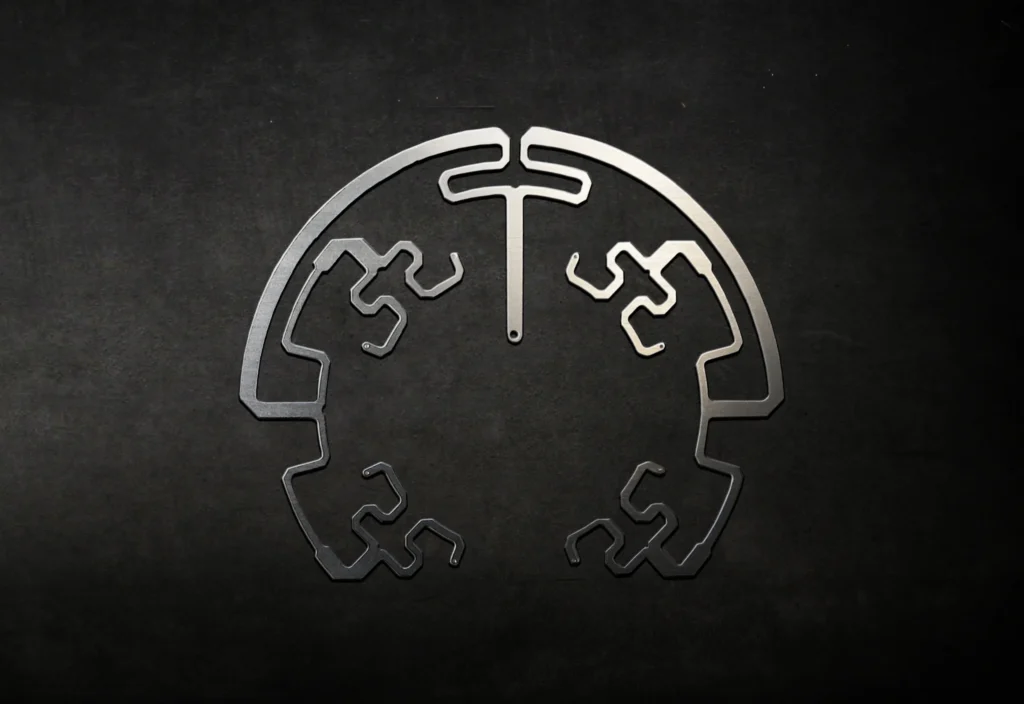
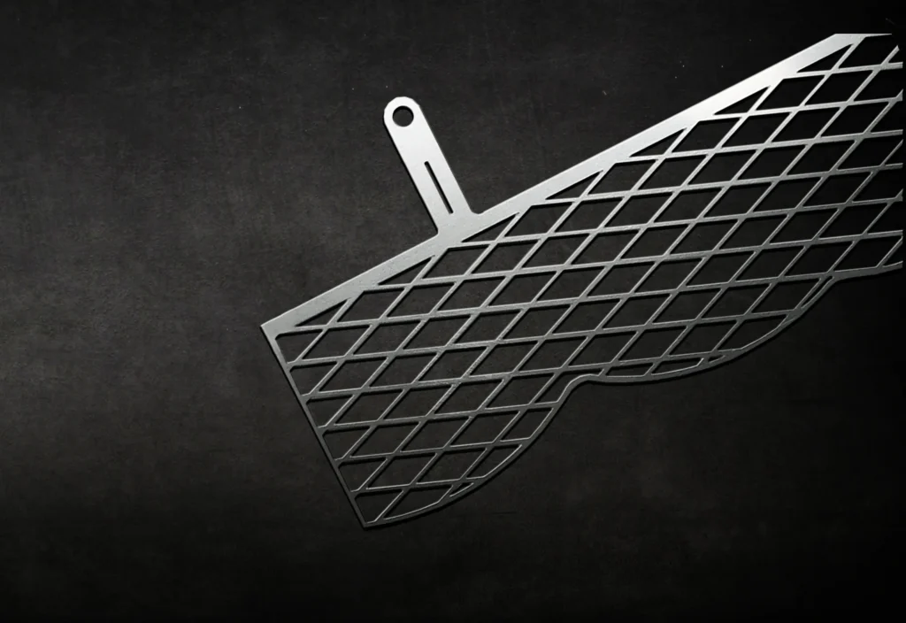
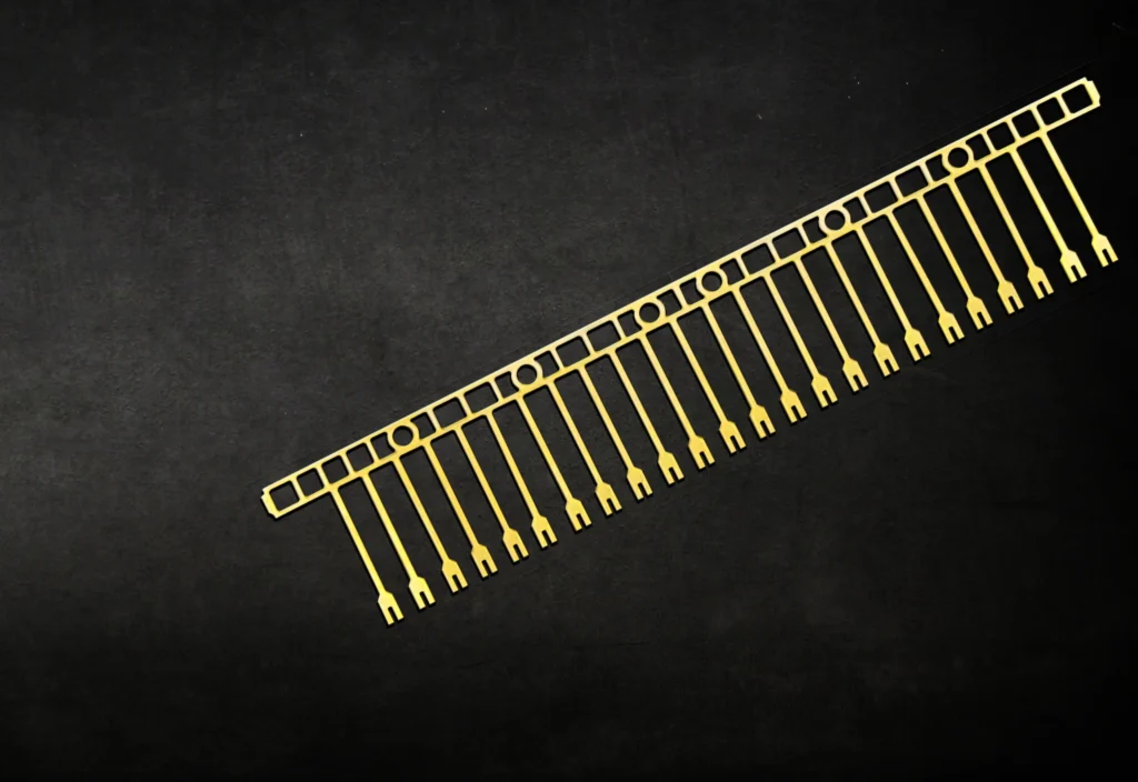
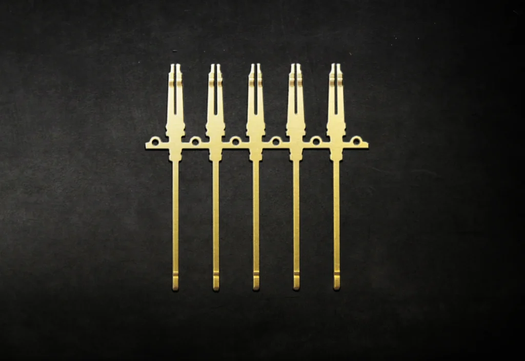
Photochemical machining enables engineers to create highly intricate geometries without the limitations associated with hard tooling.
Internal features, fine slots, perforations, and detailed patterns can be incorporated into the design without significantly increasing manufacturing cost.
Because the photo etching process uses digital imaging and film tooling rather than expensive dies, we can rapidly support:
This flexibility helps customers reduce development timelines and accelerate product launches.
PEI are experts in providing precision photochemical machining for a wide range of metals and specialty alloys, including:
This broad material selection allows engineers to optimize performance for demanding applications across various industries.
Quality is foundational to every stage of PEI’s photochemical machining workflow.
Every new part undergoes First Article Inspection (FAI) before production release. Once validated, process variables are locked to ensure repeatability across future runs.
We support strict inspection requirements for:
Packaging solutions are also tailored to customer requirements and may include:
Our team works closely with customers to ensure every component arrives protected, traceable, and ready for production use.
For decades, PEI has been a leading provider of precision photochemical machining solutions for industries requiring exacting quality, tight tolerances, and advanced manufacturing expertise.
From prototype through production, our team helps engineers overcome manufacturing challenges with precision etched components designed for performance, reliability, and scalability.
Contact us today to discuss your next precision photo chemical etching project.
We support strict inspection requirements for:
Packaging solutions are also tailored to customer requirements and may include:
Our team works closely with customers to ensure every component arrives protected, traceable, and ready for production use.
Chemical etching is a precision subtractive manufacturing process that removes metal using controlled chemical reactions rather than mechanical cutting.
Also known as photochemical etching or chemical machining, the process uses a light-sensitive photoresist to define areas of metal to be removed. After UV exposure hardens the desired pattern, chemical etchants dissolve the unprotected metal.
Because material is removed chemically — not mechanically — the process produces:
Burr-free edges
No mechanical stress
No heat-affected zone (HAZ)
Uniform material thickness
Complex geometries in thin or delicate metals
Chemical etching is widely used for precision components requiring tight tolerances and clean edge quality.
Photochemical machining (PCM) is a high-precision form of chemical etching that uses photographic imaging to control the metal removal pattern.
Chemical etching is a broad term for removing metal with chemical solutions. It may use simple masks or lower-precision methods.
Photochemical machining (also called precision chemical machining) specifically uses:
A phototool (film containing the pattern)
UV-activated photoresist
Controlled double-sided etching
This allows PCM to achieve:
Repeatable tolerances as tight as ±0.0005 inches
Micro-features and fine apertures
High alignment accuracy
Dense, intricate internal geometries
In short:
Feature | Chemical Etching (General) | Photochemical Machining (PCM) |
Pattern Control | Basic masking methods | UV photolithographic imaging |
Precision | Moderate | High (±0.0005″) |
Feature Density | Limited | Micro-features possible |
Applications | Decorative & industrial | Aerospace, medical, electronics |
PCM is the precision-engineered variant of chemical etching.
The chemical machining process removes metal through a controlled sequence of imaging and chemical dissolution steps.
The process typically includes:
1. Surface Preparation
Metal sheets are cut to size and thoroughly cleaned to remove oils, dust, and contaminants. Clean surfaces ensure strong photoresist adhesion.
2. Photoresist Application
A dry-film photoresist is laminated onto both sides of the metal sheet. This resist will define which areas remain and which will be etched.
3. UV Exposure and Developing
The sheet is exposed to UV light through a phototool or direct imaging system. Exposed resist hardens. Unexposed areas are removed during developing, revealing bare metal.
4. Controlled Chemical Etching
The sheet passes through a spray etching chamber where a carefully controlled chemical solution dissolves the exposed metal. Etch rate and chemistry are continuously monitored to maintain dimensional accuracy.
5. Resist Stripping and Finishing
Remaining resist is removed, and the finished component is cleaned, dried, and inspected.
This controlled process produces:
Burr-free edges
Flat, stress-free parts
Symmetrical material removal from both sides
Highly repeatable dimensions
Chemical milling, also known as chem milling, is the controlled removal of metal across large surface areas using chemical etching techniques.
Unlike mechanical milling, chemical milling:
Introduces no cutting forces
Produces no heat-affected zones
Maintains material integrity
Removes material uniformly
Chem milling is commonly used to:
Reduce weight in aerospace components
Thin material without distortion
Create recessed features
Maintain flatness in large panels
Because material is removed evenly from both sides, the process preserves dimensional stability.
Photochemical machining is widely used in industries requiring precision, fine features, and tight tolerances.
Common applications include:
Aerospace
Lightweight structural and avionics components requiring high accuracy and weight reduction.
Defense
Mission-critical components manufactured to strict dimensional and traceability standards.
Medical Devices
Precision instruments and implantable components made from biocompatible metals.
Electronics
EMI/RFI shielding, connectors, sensor components, and fine conductive patterns.
Telecommunications
High-precision signal routing components and thin shielding elements.
Additional industries include automotive, renewable energy, microelectronics, and specialty industrial applications.
Chemical etching produces burr-free, stress-free components without heat distortion, making it ideal for thin and precision metal parts.
Key advantages over laser cutting include:
No Heat-Affected Zone (HAZ)
Laser cutting introduces localized heat, which can cause micro-burrs or distortion. Chemical etching uses no thermal energy.
Burr-Free Edges
No mechanical force means no secondary deburring is required.
Superior Micro-Feature Capability
Chemical etching excels at:
Fine apertures
Dense internal patterns
Thin webs
High feature density
Stress-Free Components
Material is removed evenly from both sides, ensuring flatness and dimensional symmetry.
Ideal for Thin Metals
Ultra-thin foils can be etched without distortion.
For certain applications, laser cutting may be used for outer profiles while chemical etching defines internal features.
Chemical etching works on a wide range of sheet metals and specialty alloys, including:
Stainless steel (multiple grades)
Copper and beryllium copper
Brass and copper alloys
Titanium (including medical-grade)
Nickel and nickel-based alloys (e.g., Inconel)
Molybdenum
Specialty aerospace and electronic alloys
Thicknesses can range from ultra-thin foils to heavier sheet metal. Etchants are selected based on material chemistry to maintain consistent etch rates and dimensional control.
A chemical machining diagram illustrates how photoresist imaging and chemical dissolution selectively remove metal from a sheet.
A typical diagram shows:
Clean metal substrate
Photoresist coating on both sides
Phototool alignment
UV exposure hardening selected areas
Developing to remove unexposed resist
Chemical etching dissolving exposed metal
Resist stripping to reveal the finished part
The diagram visually demonstrates how protected areas remain intact while exposed areas are dissolved in a controlled manner.