In an era where the devices we rely on become smaller, smarter, and more powerful by the day, the microelectronics industry is under increasing pressure to deliver components that match the pace of innovation. From smartphones and smartwatches to autonomous systems and IoT devices, the need for lightweight, ultra-precise, and reliable components is greater than ever.
This growing demand has created a new set of challenges for manufacturers. Producing parts with sub-micron features, fine tolerances, and complex geometries at scale is not something traditional manufacturing methods were built for. As the technology sector continues to push the limits of what’s possible, engineering teams need new methods that can keep up.
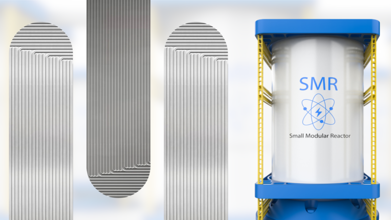
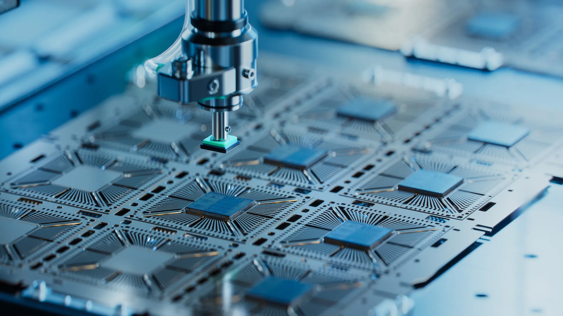
With its ability to produce highly precise, intricate geometries with exceptional material versatility and scalability, photochemical etching (PCE) has emerged as a superior process for manufacturing photonic components. And it’s easy to see why.
Photofabrication Engineering, Inc. (PEI) is a leading provider of precision chemical machining services with a reputation built on our daily dedication to perfection. With over 50 years of expertise, we stand shoulder to shoulder with our technology partners, delivering precision metal parts and components used by industry-leading computer, communications, and microelectronics manufacturers.
In this article, we explore how photo etching is transforming the technology sector and helping to push the boundaries of what’s possible.
The Limits of Traditional Manufacturing for Microelectronics
As component sizes shrink, the limitations of traditional manufacturing methods become glaringly apparent. Traditional machining methods like CNC machining, stamping, and laser cutting struggle to produce the fine features, tight tolerances, and ultra-thin profiles required for next-generation electronics.
Let’s take a deeper dive into the areas where traditional manufacturing processes fall down.
Machining Complexity at the Micro-Scale
CNC machining and laser cutting just aren’t built for the micro-scale. When it comes to creating tiny or intricate features, these methods often leave behind burrs, cause warping, or produce inconsistent tolerances. They can also damage the metal surface, which is especially problematic for electrical components where even minor imperfections can affect mating components during assembly. Plus, the mechanical stress they put on the material can seriously impact reliability, especially in high-performance electronic applications where precision is everything.
Tooling and Lead Time
Traditional methods like die stamping and machining need costly tooling and time-consuming setup, which makes them a poor fit for rapid prototyping or quick design changes, things that are absolutely vital in today’s fast-paced tech world.
Material Deformation and Distortion
The mechanical forces involved in these processes can also easily distort thin or delicate metals. That kind of damage can affect both mechanical strength and electrical performance, which are deal-breakers in microelectronics.
These aren’t just manufacturing headaches, they directly impact how well a device performs, how reliable it is, and whether it meets compliance standards. For engineers and procurement teams pushing the limits of innovation, that’s simply not acceptable.
How Chemical Etching Solves Microelectronic Challenges
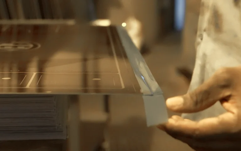
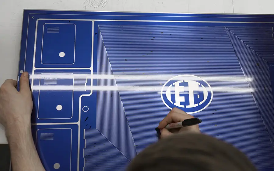
The photochemical etching process (also known as chemical etching or photochemical machining) is a subtractive manufacturing method that uses a photoresist and an acid etching solution to selectively remove metal and create highly accurate, burr-free parts.
This process is especially suitable for producing detailed components for today’s electronic devices, where material integrity and precision are critical.
Here’s why it’s ideal for microelectronic component manufacturing:
- No Mechanical Stress: Because the process is entirely chemical and non-contact, it imposes zero mechanical or thermal stress on the metal. The result? Material properties—like conductivity, tensile strength, and hardness—remain fully intact.
- Extreme Precision and Complexity: PCE can produce fine features, slots, holes, and intricate patterns with tolerances as tight as ±0.0005”. It’s an ideal solution for applications that require tighter dimensional tolerances, especially in high-density microelectronic designs. Complex geometries are easily achieved without increasing cost or complexity.
- Burr-Free, Clean Edges: The etching process leaves no burrs or deformations, reducing the need for post-processing and making parts assembly-ready for sensitive electronics.
- No Expensive Tooling: Instead of hard tooling, PEI uses photomasks that are digitally created and inexpensive to modify. This reduces time to market and costs for prototyping, design changes, and small production runs.
- Scalable for Production: Whether you’re making 10 parts or 10,000, PCE scales effortlessly. That flexibility is essential for startups and tech giants alike as they scale innovation.
In short, photochemical etching enables engineers to design without compromise, allowing performance, reliability, and innovation to come first.
Materials for Microelectronic Component Manufacturing
When it comes to microelectronics, material selection is critical. Components must combine electrical conductivity, structural integrity, and environmental resistance – all at minimal weight and thickness.
The increasing use of thin materials in compact, high-performance devices demands metals that deliver exceptional mechanical and thermal properties.
The expert team at PEI specializes in working with a wide range of metals optimized for microelectronic and medical component performance, especially for applications where thermal conductivity, high corrosion resistance, and material precision are essential. We can etch virtually any metal, from basics like copper, brass, and stainless steel to precious metals (including silver) to exotic meals such as titanium, molybdenum, and beryllium copper.
- Stainless Steel – Durable, formable, and corrosion-resistant, stainless steel is often used for structural or shielding applications. Cold-rolled stainless steels offer superior spring qualities, making them ideal for mechanical contacts and spring elements in miniaturized designs. We leverage the benefits of stainless steel and photochemically etch precision parts, including filters, fuel cell plates, stators, shims, RF shields, and surgical blades, to name just a few.
- Copper and Copper Alloys – With excellent thermal conductivity and electrical performance, copper is widely used in electrical contacts, antennas, and heat-sensitive components. At PEI, we also etch copper and zinc alloy copper components, which provide a balance of strength, conductivity, and corrosion resistance for more demanding environments.
- Beryllium Copper – Known for its high strength, superior spring qualities, and exceptional thermal conductivity, this alloy is ideal for high-reliability applications.
At PEI, we specialize in precision chemically etched microwave circuits in various metals, including brass, copper, and beryllium copper. While other manufacturers refuse to work with beryllium copper, our innovative manufacturing process safely mitigates the health hazards of beryllia dust, making us an industry leader. Plus, our process is safer than stamping, machining, or cutting the metal. - Nickel – Offers excellent corrosion resistance and is commonly used in components that require magnetic shielding or exposure to harsh environments.
- Titanium – A preferred choice in the medical industry, titanium is lightweight, biocompatible, and offers high corrosion resistance, making it suitable for medical-grade metals used in implantable and wearable devices.
- Specialty Alloys – Including Inconel, Kovar, phosphor bronze, and other engineered metals, these materials serve niche applications where performance under extreme conditions is non-negotiable.
With our industry-leading machining process, PEI boasts the unique ability to etch ultra-thin metals down to 0.0005 inches (12.7 microns), providing engineers with unmatched flexibility in creating lightweight, high-performance designs for both electronic and medical components.
Where Precision Chemical Machining Powers the Microelectronics Revolution
The need for high-precision, low-profile, and high-performance components spans across a wide range of microelectronic applications.
Here’s where PEI’s precision chemically machined metal parts are making an impact:
- Electrical Contacts and Connectors: Consistent and clean edges ensure optimal conductivity and fit, even for densely packed PCBs.
- EMI/RFI Shielding: Photochemically etched shields block electromagnetic interference, crucial for signal integrity in high-speed communications and computing. PEI offers patented shield cans with removable covers, enabling easy access for repair or component swaps.
- Battery Contacts and Flexures: With consistent spring force and conductivity, etched battery contacts are critical for compact portable, and wearable devices.
- Micro Screens and Filters: High-precision holes down to microns in diameter are used in optical sensors, medical devices, and fluidics.
- Wearable and Implantable Devices: Titanium and beryllium copper etched parts enable reliable performance in harsh biological environments, without adding bulk.
Whether for consumer electronics, aerospace communications, or implantable healthcare devices, photochemical etching is opening new doors for design and functionality.
Why Choose PEI for Metal Etched Electronic Components?
With over five decades of experience, PEI stands out as a trusted partner for the world’s most demanding technology companies. Our legacy of precision, dependability, and on-time delivery has made us the go-to team within the technology sector, especially as the demand grows for faster, safer, and more reliable solutions.
Here’s why PEI is the right choice for microelectronics manufacturing:
- Proven Expertise: Our manufacturing operators boast a 50-plus-year history of producing accurate, durable, and dependable metal parts via precision photochemical machining (PCM). Through our innovative machining process, we consistently produce a stress-free metal part with efficiency, accuracy, and cost-effectiveness.
- Unmatched Precision and Flexibility: We etch parts from 0.0005 to 0.125 inches thick, allowing customers to reduce weight without compromising durability or electrical performance.
- Specialization in Difficult Materials: PEI is one of the few companies capable of etching beryllium copper – an advanced material with exceptional thermal and electrical properties.
- Patented Solutions: Our EMI/RFI shield cans feature a patented removable cover that reduces maintenance time and risk – especially important in tightly packed or sensitive electronics.
- Fast, Reliable Turnaround: We offer industry-leading lead times with no compromise on quality, whether you need a quick-turn prototype or a large production run.
- Certifications and Compliance: We’re ISO 9001 certified and ITAR registered, ensuring compliance with rigorous quality and traceability standards critical to defense and aerospace applications.
- True Collaboration: Our team of engineers, manufacturers, and quality control professionals work closely with yours, so we understand the problem before offering the solution. That’s how innovation happens.
When performance, precision, and timing matter most, the team at PEI delivers.
Shaping the Future of the Electronics Industry
As industries race to meet growing demands for speed, miniaturization, and performance, photochemical etching is emerging as the manufacturing method of choice for advanced microelectronic components.
As the technology sector continues to push the limits of what’s possible, manufacturers need to know they’re working with a team that can consistently deliver performance and precision, without compromising on efficiency, accuracy, and cost-effectiveness.
PEI’s commitment to precision, material expertise, and collaborative partnership is empowering innovators to build the technology of tomorrow, today. Whether you’re designing the next generation of communication devices, wearable tech, or embedded systems, the path forward begins with ultra-precise components that perform flawlessly at the micro-scale. Photochemical etching is not just an alternative, it’s the enabler of next-gen breakthroughs.
At PEI, we know that technology evolves when people work together to push boundaries. And as the technology world accelerates, we’re ready to help our partners keep pace. We partner with innovators across the computer, communications, and microelectronics industries to deliver the burr-free, high-precision metal-etched electronic components that are powering the next generation of devices.
We don’t just make parts, we make partnerships.
If you have a project that demands micro-scale precision, rapid development, and trusted manufacturing expertise, PEI is ready. Our engineers, manufacturers, and QA professionals are here to answer any challenge.