At Photofabrication Engineering Inc. (PEI), we specialize in producing high-precision etched lead frames that support today’s most demanding semiconductor and microelectronic applications. Using advanced photochemical etching, we deliver lead frames that balance speed, dimensional accuracy, and design complexity, without the constraints of hard tooling.
Lead frames are essential components that bridge the gap between semiconductor chips and external circuitry. In simple terms, a lead frame provides the mechanical support and conductive pathways that allow a silicon die to interface with the outside world.
From a functional standpoint, a lead frame plays a critical role in chip-to-board electrical connection. It enables secure attachment of the die, precise alignment of conductive paths, and robust electrical connections to downstream assemblies such as printed circuit boards.
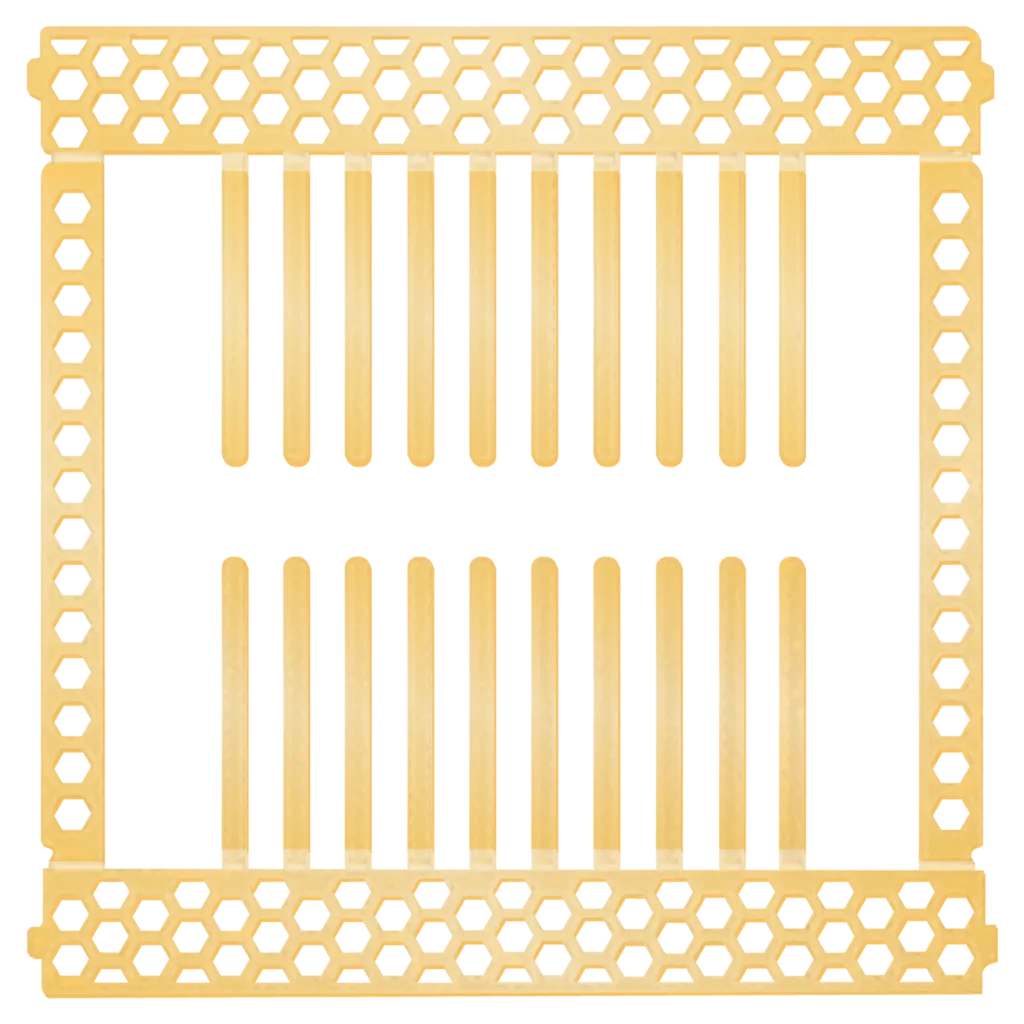
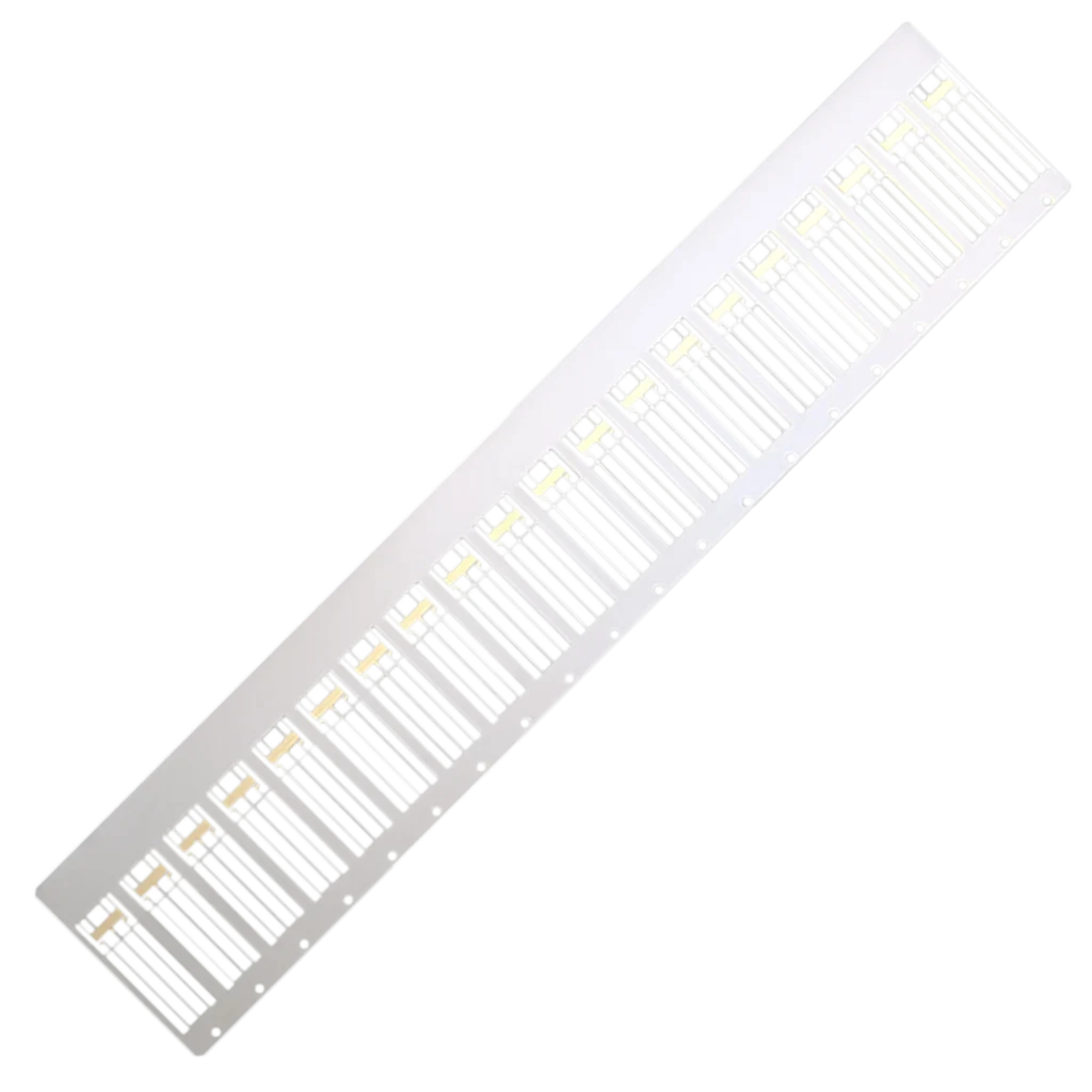
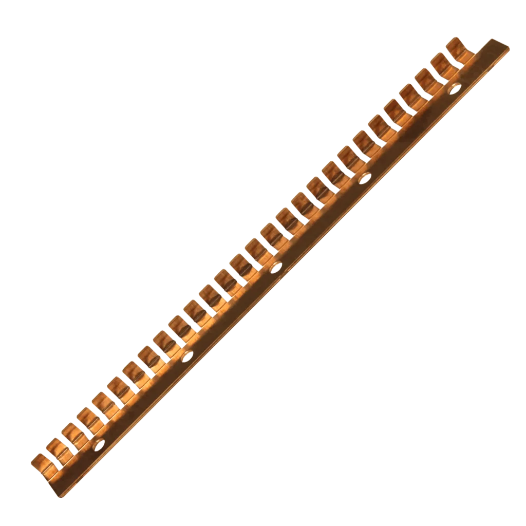
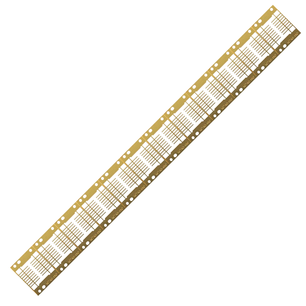
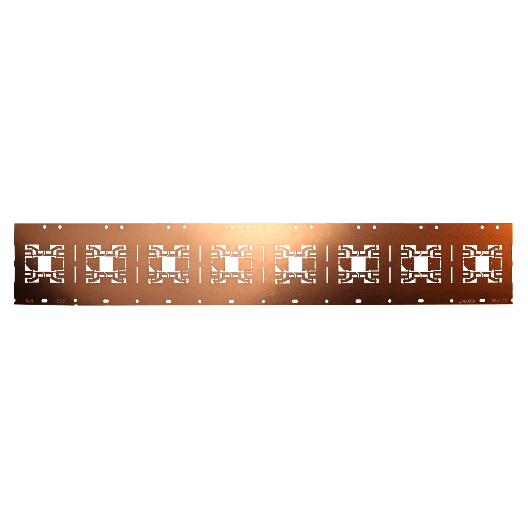
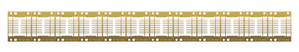
A typical lead frame consists of several key elements: the die pad supports the semiconductor die, and the inner and outer leads form conductive paths to external circuitry.
Tie bars maintain structural stability during processing and are removed or trimmed during final assembly. Together, the lead frames include features that provide a stable platform for chip packaging and long-term device performance.
Lead frames are widely used across common package styles, including QFN, DIP, TO, sensor housings, and other lead frame packages, making them a foundational component of modern electronics manufacturing.
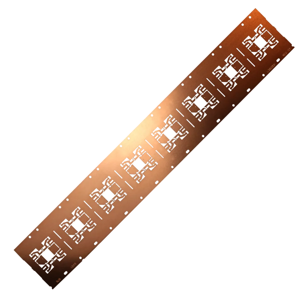
Precision in lead frame manufacturing directly influences yield, alignment accuracy, and long-term reliability throughout the semiconductor packaging process. PEI’s photochemical etching process enables extremely fine feature resolution while maintaining consistent lead frame thickness across the entire part.
Because the etching process removes material uniformly, it supports excellent electrical conductivity and predictable mechanical behavior, both of which are essential for high-density microelectronic designs. This consistency is especially important for components like integrated circuits.
PEI works with a wide range of metals selected to meet specific electrical, mechanical, and thermal requirements across microelectronic applications.
Copper alloys such as C110 and C194 are commonly used due to their excellent electrical conductivity and higher thermal conductivity, making them ideal for applications where efficient heat flow away from the die is essential. Iron nickel alloys, including Alloy 42 and Kovar, are often selected for their closely matched thermal expansion coefficient when interfacing with silicon or ceramic packages, helping reduce mechanical stress during thermal cycling.
Stainless steels and other specialty materials are also available for applications requiring added strength, environmental stability, or enhanced corrosion resistance. Each material option is evaluated based on the intended operating environment, assembly method, and performance requirements to ensure optimal results.
PEI has decades of experience fabricating lead frames from copper and these materials:
Photochemical etching offers significant advantages over stamping and CNC machining for precision lead frames – particularly as designs become smaller and more complex.
The benefits of precision chemical machining for lead frames include the ability to fabricate precise parts with intricate geometries and accurate patterns without inducing mechanical stress on the metal structure. Because there is no physical tooling contact, etched parts remain flat and free of distortion.
Etched lead frames are compatible with advanced assembly techniques, including traditional wire bonding and flip chip configurations, where edge quality and positional accuracy are critical to long-term device reliability.
Key advantages of the etching process include:
Etched lead frames are particularly well-suited for applications involving wire bonding, where edge quality and dimensional consistency directly affect assembly yield and long-term reliability.
Effective thermal management is a critical requirement in modern semiconductor design, particularly as power densities increase and device footprints shrink. Lead frames play a central role in enabling efficient heat transfer from the active device to the surrounding environment.
Material selection, geometry, and surface finish directly influence overall thermal conductivity and heat dissipation capability. Etched lead frames provide consistent cross-sectional profiles that support predictable thermal paths, helping maintain stable operating temperatures and protect sensitive components.
Optimized lead frame designs contribute to improved thermal performance without compromising electrical or mechanical integrity, supporting long-term reliability in demanding applications.
For more than 50 years, PEI has supplied lead frames to leading manufacturers in the semiconductor and technology sectors. Our etched components are used across a wide range of industries and applications, including:
PEI also offers value-added options such as plating, part marking, custom tabs, and integrated tie bar designs to support downstream assembly and identification requirements.
Selecting the right manufacturing partner is critical to the success of any microelectronic program. PEI combines deep process expertise with responsive, U.S.-based production to support customers from early development through full-scale manufacturing, ensuring consistent electrical performance across production runs.
Our in-house engineering team works closely with customers to refine designs, select appropriate materials, and optimize manufacturability for reliable signal transmission in demanding semiconductor applications. With decades of experience supporting complex manufacturing processes for microelectronic components, PEI delivers solutions tailored to real-world production requirements.
ISO-certified quality systems and rigorous inspection protocols ensure every lead frame meets exacting standards for accuracy, consistency, and long-term reliability.
With a history of engineering excellence, PEI is among the top companies providing photochemically etched metal parts and components for various critical industries.
With ISO-9001:2008 and AS9100 certifications, PEI was also granted certification under the International Traffic in Arms Regulation (ITAR) in 2010, enabling it to provide weapon system components and accessories in compliance with the Code of Federal Regulations implemented by the U.S. Department of State.
Our rigorous inspection processes and testing procedures ensure that every product we produce meets stringent accuracy, reliability, and performance standards.
Whether you’re developing a new semiconductor device or optimizing an existing package, PEI delivers etched lead frames engineered for performance, reliability, and scalability.