As electronic devices grow faster, smaller, and more densely packed, they also become more vulnerable to a growing threat: electromagnetic interference (EMI). Whether it’s an aerospace navigation system or a consumer wearable, today’s electronics operate in crowded signal environments where even minor EMI can compromise performance, reduce lifespan, or trigger regulatory failure.
The best defense against these risks? Smart EMI shield design, done early, with performance in mind.
The design phase is where engineers have the most control over shielding effectiveness. Every decision can affect how well a shield blocks or redirects harmful electromagnetic radiation and electromagnetic waves.
At Photofabrication Engineering, Inc. (PEI), we’ve spent over 50 years perfecting the art of manufacturing precision EMI shielding enclosures. From PCB cans to multi-cavity enclosures, PEI partners with engineers across aerospace, medical, RF, and defense sectors to fabricate high-performance, photochemically etched EMI shields.
In this article, we explore the fundamentals of EMI shielding design, key material and process considerations, and how to prototype smarter with PEI.
The Impact of Electromagnetic Interference
Electromagnetic interference is the unwanted disruption of an electronic system by external or internal electromagnetic fields. These disturbances can corrupt signals, degrade performance, or even shut down devices.
The key impacts of EMI include:
- Safety Risks – EMI can disrupt critical systems in medical devices and military equipment, risking patient safety or mission failure.
- Signal Loss or Corruption – EMI can cause data loss or introduce errors in communication systems, sensors, and processors.
- Regulatory Failure – Devices that emit or receive excessive EMI may fail FCC, CE, or MIL-STD testing.
- Higher Costs – EMI issues caught late require expensive design rework, part replacement, or even product recalls.
Sectors including aerospace, RF communications, telecommunications, automotive, defense, and medical electronics are particularly vulnerable to EMI, as even minor interference can lead to serious performance or safety consequences.
Why EMI Shielding Design Matters
Well-designed EMI shields do more than block interference; they build performance and reliability into the product from the start.
Benefits of effective EMI shielding:
- Prevents data corruption and signal degradation
- Improves reliability, longevity, and user safety
- Reduces the risk of regulatory compliance failure
- Protects sensitive signal lines and critical electronic components
- Minimizes internal and external EMI emissions
For systems involving cable shielding, power management, or RF communication, shielding isn’t optional; it’s essential.
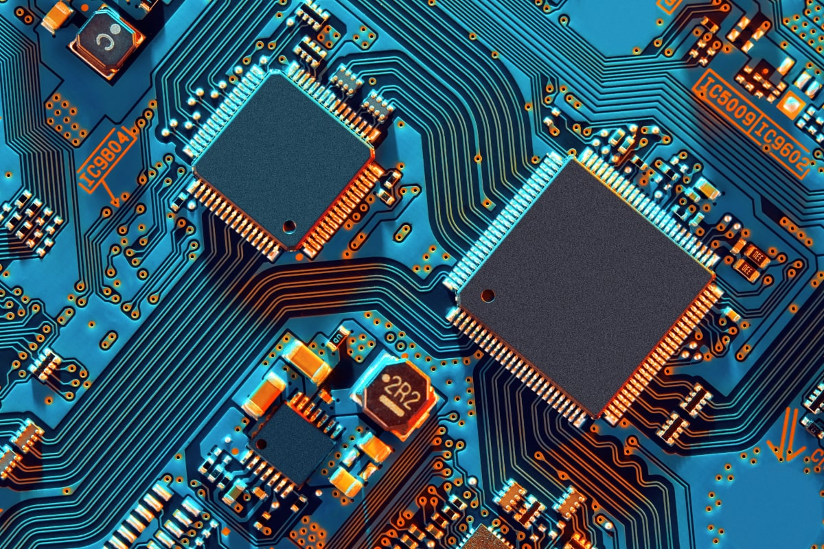
Common EMI Shield Types
Designing EMI shielding begins with choosing the right format for your application.
Here are the most common types:
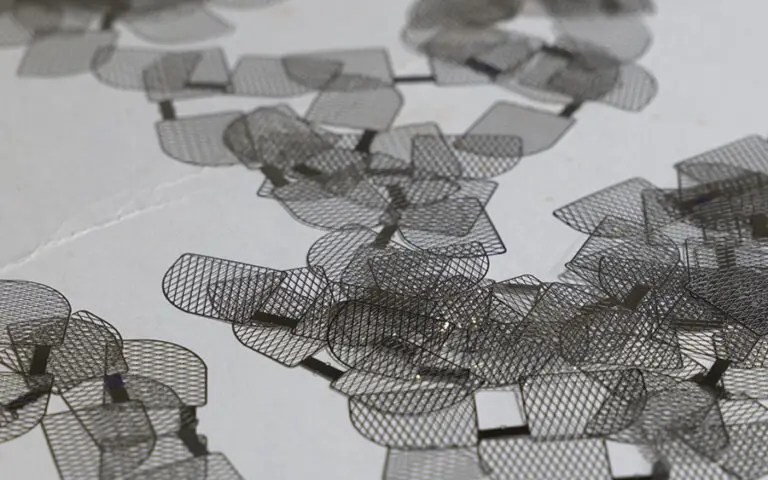
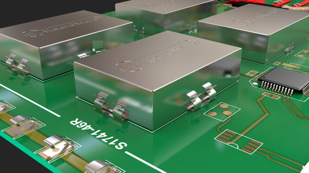
- PCB Shielding Cans – Single- or two-piece enclosures that sit over board-level components.
- Board-Level Enclosures – Full shields protecting subassemblies or critical zones.
- Multi-Cavity Shields – Used for devices with multiple isolated RF paths or signal clusters.
- Surface-Mount vs. Through-Hole – Choice depends on board layout, grounding scheme, and production method.
- Clip-On or Soldered Tabs – Design affects rework, replacement, and assembly time.
Each type requires different design trade-offs based on performance, cost, board layout, and enclosure design.

Design Considerations for Precision EMI Shielding Enclosures
Designing an effective EMI shield means balancing electrical performance with mechanical practicality.
Key considerations during the design phase include:
1. Material Selection
- Copper – Excellent shielding material with high conductivity; requires surface protection.
- Nickel Silver – Great for corrosion resistance, aesthetic finish, and good conductivity.
- Stainless Steel – Strong and durable; less conductive but good for structural shielding.
All materials must be compatible with conductive coatings, conductive gaskets, and other board-level features.
2. Geometry & Openings
- Louvers, Vents & Cutouts – Required for heat dissipation, airflow, or connector access. Design to minimize leakage.
- Slot Spacing – Openings should be <1/20 of the shortest target wavelength to avoid resonance or signal escape.
3. Mounting Method
- Soldered Tabs or Pins – Ensure stable grounding and permanence.
- Clip-on Shields – Allow easy removal, rework, or replacement without desoldering.
4. Wall Height & Thickness
Wall dimensions should accommodate the surrounding components and the expected field strength. PEI can fabricate shields from metal sheets as thin as 0.001”.
5. Grounding and Fit
Electrical continuity is critical. Maintain strong, consistent contact between the shield and PCB ground plane to avoid gaps or deformation.
6. Thermal Management
Include design features like vent holes, thermal gap fillers, or louvers to prevent overheating.
7. Early Prototyping
Etched shields allow rapid iteration. Engineers can test performance without committing to costly tooling, a major benefit when controlling EMI under tight timelines.
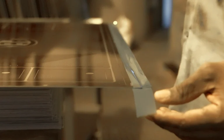
Why Etching Is Ideal for EMI Shielding
The team at PEI specializes in precision photochemical etching, a manufacturing process uniquely suited for producing high-precision EMI/RFI shielding components.
Unlike mechanical cutting or stamping, etching enables the creation of intricate geometries, fine apertures, and thin-walled features without introducing stress, distortion, or burrs. This makes it ideal for sensitive electronic assemblies where dimensional accuracy and shielding performance are critical.
Here’s why chemical etching is the superior manufacturing process:
- Tight Tolerances – Precision down to ±0.0005″, ideal for snap-fit, press-fit, or surface-mount applications.
- Burr-Free Features – No mechanical distortion = no secondary deburring.
- Zero Tooling Stress – Unlike stamping, etching introduces no stress or deformation to the part.
- Custom Markings – Easily add part numbers, logos, or batch info during the etching process.
- Complex Geometries – Create fine apertures, intricate designs, and multi-aperture shields with ease.
- Mixed Volumes – Perfect for both prototypes and full production runs.
At PEI, our etching process supports features that would be difficult or impossible to achieve through stamping, punching, or CNC alone.
How PEI Supports EMI Shielding Design and Performance
At PEI, our design philosophy is built on collaborative engineering support. We don’t just build shields – we help design them. At PEI, our engineers work directly with customer design teams to review layouts, materials, grounding methods, and venting. Our goal is to enhance shielding performance before fabrication begins.
Through in-house collaboration between our engineering, tooling, and manufacturing teams, we deliver EMI shields that meet exact design intent and manufacturability requirements.
When smart people work together, they solve complex EMI problems faster—and build better parts.
PEI’s In-House Manufacturing Advantages
When you work with the trusted team at PEI, you gain access to a vertically integrated model that delivers:
- Rapid quoting and prototyping
- Short lead times
- Certified production under ISO 9001:2015 and AS9100
- Strong relationships with aerospace, telecom, and medical OEMs
- Wide range of in-stock shielding materials
From concept to coating, we support every step.
Build Shielding Into the Design
Designing EMI shielding isn’t just about blocking interference; it’s about engineering confidence into your product from the start.
By understanding key design principles, selecting the right conductive materials, and choosing the right fabrication method (Photochemical etching is the clear winner), engineers can design EMI shields that meet today’s performance, cost, and compliance demands.
At PEI, we specialize in producing high-precision EMI shielding enclosures that protect critical electronic components across industries where performance and reliability are essential. As a leading precision etching company, we consistently deliver custom photochemically etched EMI shields with unmatched accuracy and speed.
Let’s work together to reduce EMI, improve reliability, and build better systems.
Ready to prototype or quote your next EMI shielding solution?
Let’s work together to create a custom shield for your PCB or enclosure.