In the beginning…
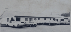
 Photofabrication Engineering, Inc. (PEI) was established in October 1968 in Holliston, MA in order to supply the fast-growing semiconductor and computer peripheral manufacturers in the Boston area with metal precision parts quickly and inexpensively. Our first building was only 4,000 square feet.
With the process of photochemical machining (PCM), the tooling needed to produce precision parts is essentially a low-cost, easily produced film that allows companies to move quickly through the product development cycle. As word of this innovative technology spread throughout the industry, PEI was on its way, becoming a proven source for precision parts.
 Also, with PEI’s proximity to the Rhode Island costume jewelry world, jewelry manufacturers quickly became aware that the photochemical machining (PCM) process was a perfect fit for their needs. They could manufacture findings quickly, and did not have to incur the high costs required by metal stamping. This lead to the creation of PEI’s Decorative Products Division in the mid-1970’s.
Moving into the 1980’s

As PEI’s product lines and manufacturing capabilities expanded, the Board of Directors searched for a new president to take the company into the 1980’s and beyond.
In 1977, William M. Lehrer was hired from Oak Industries to become president of PEI, bringing his vast engineering experience and outstanding educational background with him. Bill earned his Bachelor of Science degree in Chemical Engineering and his Master’s degree in Metallurgical Engineering from Rensselaer Polytechnic Institute.
While working at Raytheon Company, he received a Master’s degree in Business Administration from Northeastern University.
Bill was the perfect fit for a company that manufactures etched metal precision parts with sophisticated chemistry.
In the following years, PEI grew steadily, mainly because of its focus on providing the highest level of quality, which continues to be of the utmost importance to the management team. In 1983, management realized that more space and equipment would be needed, and decided to build a state-of-the-art facility dedicated to the PCM process in Milford, MA.
A State-of-the-Art PCM Facility

PEI broke ground in 1983 in Milford, Massachusetts’s Granite Park. Once the facility was completed in 1984, design and manufacturing equipment was installed; a four-stage metal hydroxide precipitation process area for waste treatment was built; and the corporate, sales, and marketing offices were relocated to Milford.
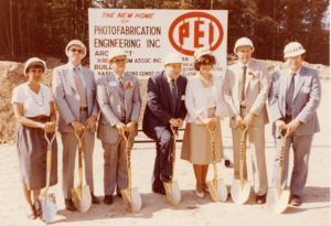 The facility’s 40,000 square feet allowed PEI to continue its growth and develop new product lines and technology. With this building, PEI became the world’s largest photoetching company under one roof.
Industry Expansion in 2010
Today Chip Lehrer, President of PEI, continues the expansion of PEI’s Precision Products Division by manufacturing mission critical parts for most technology-driven industries. The company etches almost all metals, including Stainless Steel, Copper, Brass, Kovar, Sterling Silver, Beryllium Copper, Nickel Silver, Titanium, Zirconium and other standard and specialty metals and alloys. PEI is also the industry leader in Titanium etching for a wide variety of applications, including medical implants and fuel cells.
 PEI’s Decorative Products Division manufactures custom Brass ornaments, collectibles, and other items for museum stores, foundations, large and small non-profits, universities, and companies looking to recognize their customers and/or employees.
PEI has developed a series of programs to help non-profits raise revenue for their organizations, offering assistance with marketing, design, and fulfillment. The programs allow non-profits to create a new revenue stream that they can rely on year after year. PEI now has hundreds of customers that look forward to the New Year and their new ornament design.